In today’s tech landscape, data is the foundation of innovation. Efficient and accurate data acquisition is critical for scientific research, industrial automation, medical diagnostics, and more — and that’s where Data Acquisition (DAQ) systems come into play. Among various DAQ technologies, systems based on Field-Programmable Gate Arrays (FPGAs) have garnered significant attention for their exceptional performance and flexibility.
An FPGA is like a chip that can be “reshaped” to meet specific requirements. It enables high-speed, parallel processing of large volumes of data, achieving ultra-low latency and high performance that traditional processors often struggle to deliver. This makes FPGAs a powerful choice for DAQ applications that demand high throughput and precise timing control.
However, unlocking the full potential of FPGAs comes with its own set of challenges. In this article, we’ll explore the key obstacles on the road to high-performance data acquisition.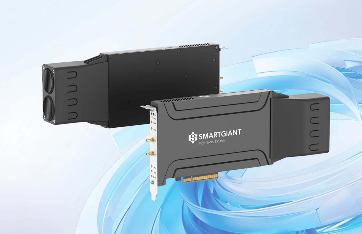
1. Advantages of FPGA-Based DAQ
Before we delve into the challenges, let’s first take a quick look at the compelling advantages of FPGA-based DAQ systems:
- Unmatched speed and parallelism: FPGA logic units can work simultaneously, like thousands of miniature processors operating in parallel, effortlessly handling data rates in the range of gigabytes or even tens of gigabytes per second.
- Millisecond-level low latency: With direct hardware-level data routing, FPGAs avoid the delays typical of software-based forwarding—critical for real-time control and response.
- Highly customizable: The programmable nature of FPGAs allows hardware logic to be tailored to specific application needs, achieving optimal performance-to-power ratios.
- Flexibility and upgradability: Once deployed, FPGAs can be reprogrammed to upgrade features and extend the lifecycle of a system.
2. Six Challenges of Implementing High-Performance FPGA-Based DAQ
Despite its significant advantages, implementing an FPGA-based DAQ system is not without challenges. Key obstacles include:
- Hardware Design & Debugging:
Designing FPGA boards is highly complex, requiring precise control of high-speed signal integrity (such as impedance and trace length), stable power delivery, and effective thermal management. This demands deep expertise in hardware engineering. - HDL Programming:
FPGA development involves using hardware description languages like Verilog or VHDL for parallel system design. Managing a large number of concurrent tasks can be difficult, and HDL code is often extensive, hard to debug, and less readable and maintainable. It requires a different mindset compared to traditional software development. - Hardware-Software Co-Design:
Achieving a smooth integration between FPGA firmware and host software is essential. This includes implementing communication interfaces (e.g., PCIe, Ethernet, USB), designing protocols, developing drivers, and providing APIs to ensure reliable and efficient data transfer. - Testing & Verification:
The system’s complexity calls for rigorous validation, including functional simulation, timing verification, hardware-in-the-loop (HIL) testing, and stress testing to guarantee stability and reliability. - Talent & Learning Curve:
FPGA development requires strong knowledge in digital circuits, signal processing, FPGA architecture, and toolchains. The steep learning curve and shortage of experienced engineers increase both development cost and time. - Cost & Project Timeline:
Initial investment can be high due to the cost of high-end FPGAs, EDA tools, and IP cores. The development cycle is often lengthy due to complex design and validation processes. However, the resulting performance, reliability, and customization capabilities make it a valuable long-term solution for demanding applications.
3. Smartgiant’s Solutions
At Smartgiant, we understand that experience and expertise are essential for overcoming these challenges. As a company dedicated to delivering high-performance DAQ solutions, we:
- Have a seasoned expert team: Our engineers bring years of experience in FPGA design, high-speed hardware, and embedded software development.
- Follow a mature development process: From requirements analysis and system design to implementation, firmware development, and verification, we adhere to standardized workflows that ensure quality and reliability.
- Utilize advanced tools and technologies: We leverage industry-leading FPGA tools, simulation platforms, and testing equipment.
- Offer customized solutions: We provide tailored FPGA-based DAQ systems to meet specific customer requirements.
- Continuously innovate and learn: We keep pace with the latest developments in FPGA and DAQ technologies.
Most importantly, we’ve distilled our expertise into a portfolio of user-friendly, high-performance FPGA-based DAQ products—empowering customers to harness the power of high-speed data with ease.
Let’s take a look at three of Smartgiant’s flagship FPGA-based DAQ products, covering diverse use cases and offering powerful technical features.
3.1 FPGA Architecture: The Heart of Data Acquisition
Smartgiant’s DAQ architecture includes an Analog Front-End (AFE), Analog-to-Digital Converter (ADC), FPGA SoC, and trigger modules:
- AFE Signal Conditioning: Amplification and filtering ensure signal stability. Supports input ranges from ±0.9V to ±10V for compatibility with various signal sources.
- ADC Digitization: Supports resolutions from 8 to 24 bits and sampling rates from 50 KSPS to 5 GSPS, covering applications from slow, high-precision signals (e.g., medical) to fast, wideband signals (e.g., radar).
- FPGA Parallel Processing: Based on Xilinx Zynq 7000 (general use) and Zynq MPSoC (high-speed) series, integrating ARM processors with programmable logic. Supports real-time signal processing (e.g., FFT), data buffering, and custom algorithm acceleration.
- Trigger Mechanism: Supports internal, external (level/edge), and software triggering to ensure picosecond-level synchronization under complex conditions.
3.2 Three Core Products: Tailored for Diverse Needs
Smartgiant’s FPGA-based product lineup addresses embedded, high-speed, and industrial edge scenarios:
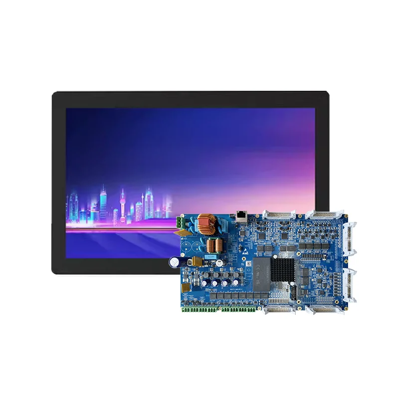
3.2.1 High-Speed DAQ Module: The “Precision Probe” for Embedded Applications
- Specs: Dual-channel, 12-bit ADC, 125 MSPS sampling rate, 30 MHz bandwidth, ±0.9V input range. Powered by Xilinx Zynq 7000 (e.g., XC7Z020), with 1 GB DDR3L and 4 GB eMMC. Can operate standalone or with a controller.
- Highlights: Low power (<5W) and compact design ideal for portable devices or distributed sensor networks. FPGA-enabled flexibility supports real-time filtering and feature extraction, such as anomaly detection in battery charging curves in new energy systems.
- Use cases: ECG monitoring, motor vibration analysis, aerospace sensor fusion.
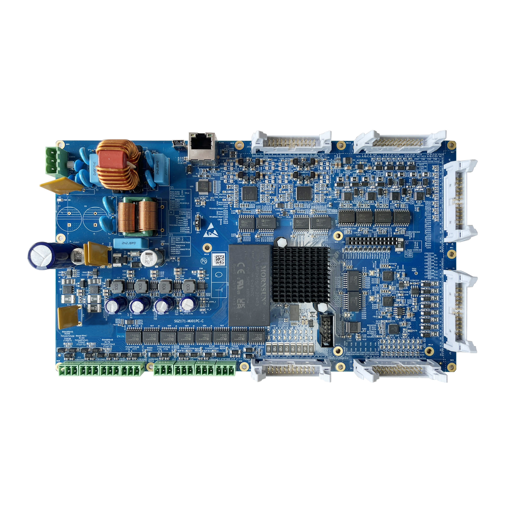
3.2.2 SG1227 PCIe High-Speed DAQ Card: The “Time Slicer” for Fast Signals
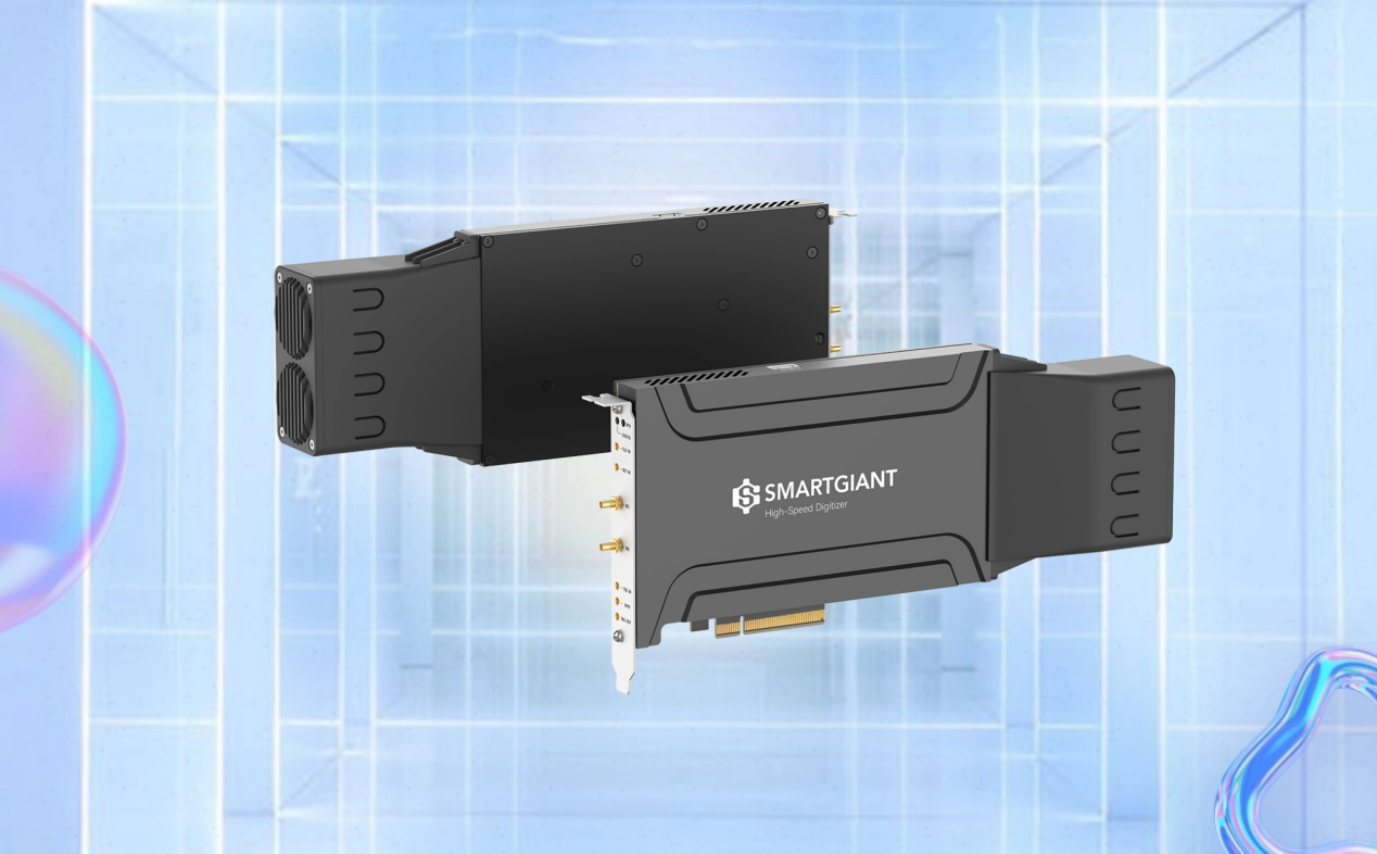
- Specs: 8-bit dual-channel, up to 5 GSPS (interleaved), 500 MHz bandwidth, ±5V input range (9 levels). Built with Xilinx Kintex UltraScale+ XCKU040, with 4 GB DDR4, 32 MB Flash, and PCIe 3.0 x8 interface (8 GB/s throughput).
- Highlights: Ideal for ultra-fast signals like LIDAR or semiconductor tests. ENOB 6.2@10 MHz. Strong sync capabilities with external 2.5 GHz clock and versatile trigger sources, achieving picosecond-level timing.
- Use cases: Laser detection, mass spectrometry, wafer defect localization.
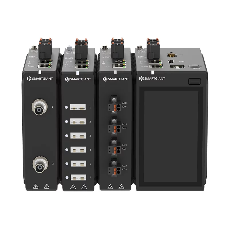
3.2.3 SG2168 High-Speed DAQ Box: The “Smart Hub” at the Industrial Edge
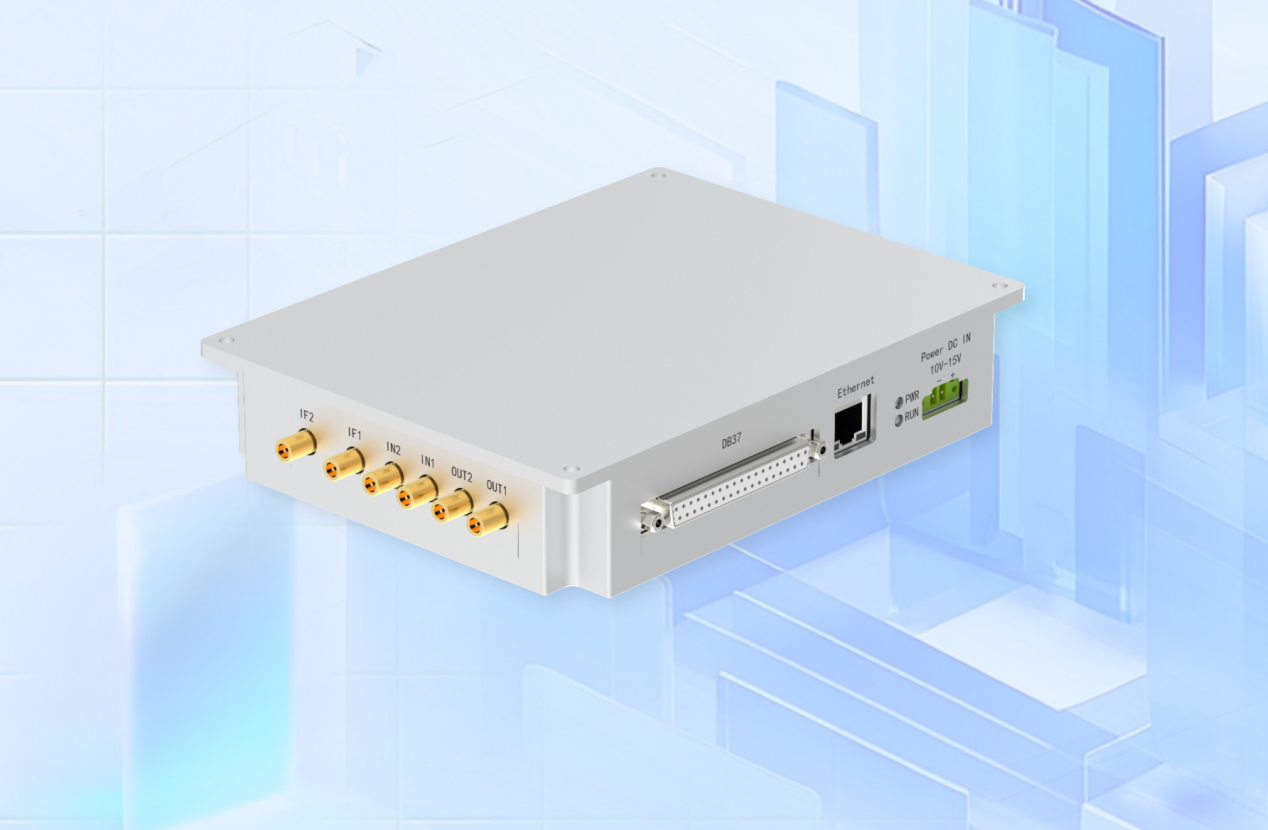
- Specs: Dual 14-bit ADCs, 500 MSPS sampling, 200 MHz bandwidth, ±1V input, AC-coupled. Uses Xilinx Zynq UltraScale+ MPSoC (e.g., XCZU4EG), integrates Gigabit Ethernet, CAN, RS485, and supports -40°C to 85°C operation.
- Highlights: ARM + FPGA architecture enables local processing (e.g., noise reduction, harmonic analysis) to reduce 90% of redundant data transmission. Industrial-grade reliability with a metal shielded enclosure, power redundancy, and EMI resistance.
- Use cases: Industrial machine monitoring (e.g., motor fault prediction), real-time signal analysis in medical devices.
3.3 Technical Innovations: Addressing Three Core Development Challenges
Smartgiant lowers the development barrier for FPGA-based DAQ through engineering optimizations, toolchain integration, and robust validation:
- Standardized hardware design: System-on-Module (SOM) integrates power and clock circuits. Four-layer boards with ±5mil trace length control and differential signaling ensure distortion <0.1% at 500 MHz.
- Improved development efficiency: Graphical tools and IP libraries with cross-platform support (LabVIEW/Python) shorten development time by 40–60%.
- Reliable validation: All products undergo 12-hour stress tests, -40°C to 85°C thermal cycling, and EMC tests, ensuring >100,000 hours of stable industrial operation.
4. Seize the Opportunity: Unlock New Value in Data Acquisition
High-performance data acquisition is a driving force behind next-generation technologies. FPGA-based DAQ systems are at the forefront of this transformation. We’ve explored both their tremendous potential and the technical, engineering, and talent-related challenges they present.
At Smartgiant, our mission is to turn the powerful capabilities of FPGAs into reliable, easy-to-use, high-performance DAQ systems. Our products are a testament to our technical expertise—and a direct response to real-world demands.
In today’s data-driven world, the ability to capture data in real time and with precision is key to staying ahead. If you’re facing high-performance DAQ challenges or want to unleash the full potential of FPGA in your applications, reach out to Smartgiant. Let’s work together to transform cutting-edge technology into your competitive advantage—and let data fuel your innovation and success.